What's New @ GT in Packaging? Innovative EMI Isolation Structures
Georgia Tech and its industry partners have developed the most advanced package-level electromagnetic interference (EMI) shielding structures for emerging highly-miniaturized System Packages.
Electromagnetic interference (EMI) is defined as unwanted electrical or magnetic coupling between components in a module or system. Such coupling or cross-talk results to performance degradation and electromagnetic compatibility issues. With increased multi-functional integration and miniaturization of emerging consumer, IoT, and automotive electronics, component-level EMI shielding has become extremely important to prevent undesired electromagnetic (EM) coupling.
EMI noise in traditional modules with large components is shielded by metallic cans or creating physical separation between them. Shielding with conformal metal coatings on overmolded packages has also been demonstrated. Component-level shielding has been developed with integrated via-based shields inside packages.
In contrast to the prior approaches described above, Georgia Tech team has recently pioneered innovative multi-layered structures for more effective EMI shielding. In the near field region, magnetic fields, generated from sources such as power inductors and transformers, have lower wave impedance and hence are difficult to be shielded with blanket sheets of a few micron thickness. To address this challenge, unique thin magnetic-nonmagnetic multi-layered structures, which lead to high shielding effectiveness, are developed. The primary shielding mechanism for such thin multi-layered shields is the multiple reflections that occur at interfaces between magnetic and conductive thin layers because of impedance mismatch. Furthermore, by employing copper as a conductive material, absorption loss also contributes to high shielding effectiveness.
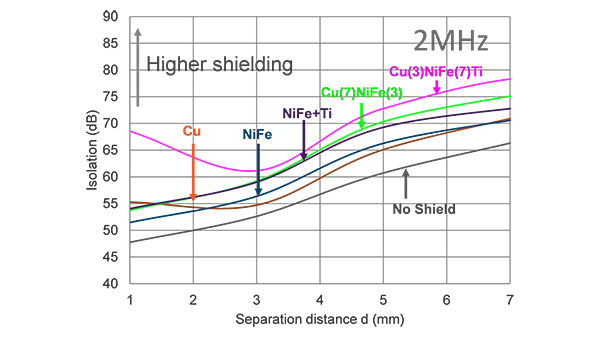
The Georgia Tech team, in partnership with Tango Systems, has demonstrated this concept with ultra-thin (< 5 micron) multi-layered shield composed of copper (Cu), titanium (Ti), and nickel-iron (permalloy) for noise suppression of 100 kHz to 100 MHz from DC-DC converters as an example. In this frequency range, such multi-layer shields placed between two magnetic coils show higher isolation or less near-field inductive coupling than traditional shielding materials such as copper or nickel films. Multi-layered structures composed of Ti, Cu, and NiFe showed 59 dB isolation, or more than 20 dB shielding effectiveness, much greater than NiFe-Cu shield or the NiFe-Ti multi-layered structures. This approach is now extended for further improvement in shielding effectiveness performance by employing oxide layers such as alumina within the multi-layered structures.
In addition to those multi-layered shielding materials, Georgia Tech team has also been pioneering package-integrated copper via-trench structures for component-level shielding between sensitive RF components. Such shields are now custom-designed for isolation between transmission lines, RF inductors, also RF power amplifiers. Since undesired EM coupling occurs both from above and below the substrates, innovative trench shielding structures with through-substrate vias or micro-vias are designed and demonstrated with 2-4 GHz shielding of above 65 dB even with component separation of below 0.5 mm. Georgia Tech is now extending these trench-via array and multi-layered conductor structures to 5G and other mm-wave modules in the frequency range of 28 GHz to 39 GHz.
This research is being performed in partnership with a large global team of material and tool companies and with support from several on-site industry engineers at Georgia Tech.
This project is part of Georgia Tech industry consortium in System Scaling which includes about 40 end-user and supply chain companies and RF module companies.
About the Authors
Atom Watanabe is an ECE student pursuing his PhD under the advisement of Prof. Rao Tummala. His research focus is on 5G modules with advanced shielding structures. atom@gatech.edu
Dr. P.M. Raj is the Program Manager for Integrated Passive and Actives as well as High-Temp Electronics at Georgia Tech PRC. raj@ece.gatech.edu
Prof. Rao Tummala is Joseph. M. Pettit Chair Professor in ECE and MSE and Director of Georgia Tech’s Packaging Research Center. rao.tummala@ece.gatech.edu.